English
 中文简体
中文简体 русский
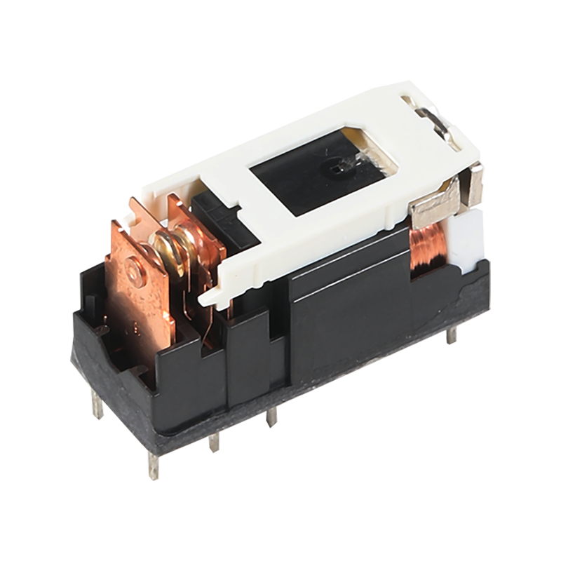

Two circuit boards joining inside one enclosure need more than a row of matching pins. The gap between them, the header height and the way power and signal lines share the same connector body all come from a single decision made early in the design: how far apart the two boards need to sit. Board To Board PCB Connectors are built around that stacking height early, and the pin layout follows from it.
Stacking height comes before pin count
A mezzanine board mounted parallel to a main board, a common layout inside compact electronics, needs a connector that holds the two boards at a fixed, known distance apart. Board To Board PCB Connectors come in a range of stack heights for exactly this reason, since the same pin count and pitch can be built into a header that holds the boards close together or one that leaves more clearance for taller components on the main board underneath.
Getting the stacking height wrong on Board To Board PCB Connectors causes problems that show up only once the enclosure is assembled. Too little clearance and a component on one board presses against the other board or its housing. Too much clearance and the connector adds unnecessary height to a design meant to stay compact. A PCB connector family that offers several stack heights on the same pin layout lets a design team change board spacing without redesigning the header footprint on either board.
Keeping power and signal apart on one header
Many board-to-board applications carry both power and signal lines across the same connection, and how those two types of lines sit relative to each other inside the connector body affects performance more than pin count alone. Placing power pins together in their own block, separate from the signal pins, keeps the switching current on the power side from inducing noise into nearby signal lines. Board To Board PCB Connectors designed with this separation in mind group power contacts at one end of the header or on a separate row, rather than interleaving them with signal pins across the same row.
Contact size on Board To Board PCB Connectors follows the same logic. Power pins usually carry a heavier gauge contact than a signal pin needs, since higher current calls for more contact area to keep resistance and heat manageable at the connection point. A PCB connector built with mixed contact sizes on one header lets a single connector carry both jobs without oversizing every pin to match the heaviest load.
Mounting method and solder joint reliability
How Board To Board PCB Connectors attach to the board affects how well the connection survives vibration over the life of the product. Surface-mount connectors solder directly to pads on the board surface, which suits automated assembly lines well but places more reliance on the solder joint alone to hold the connector in place under mechanical stress. Through-hole connectors pass their pins through the board and solder on the opposite side, which gives a mechanically stronger joint that better resists the repeated flexing a board can see in a vehicle or industrial setting.
Board To Board PCB Connectors intended for equipment that sees regular vibration often favour the through-hole mounting style for this reason, even though it adds a manual or semi-automated step that surface-mount assembly does not need. A connector aimed at consumer electronics, where vibration exposure is minimal, can rely on surface-mount attachment without the added assembly step, since the solder joint alone provides sufficient reliability in that lower-stress environment.
Specifying a board-to-board connector
Buyers selecting Board To Board PCB Connectors for a new design can specify stack height, pin count, power-to-signal ratio and mounting method together, rather than starting from pin count alone and working backward. Listing all four factors up front lets a factory confirm whether an existing header family covers the requirement or whether a custom stack height is needed for the specific enclosure being designed.
A PCB connector family built around a shared pin pitch but offered in several stack heights and both mounting styles gives a design team room to adjust the physical layout of a product without changing the underlying Board To Board PCB Connectors interface, which keeps the change contained to mechanical spacing rather than triggering a full electrical redesign. That flexibility matters especially when a product line spans several enclosure sizes built around the same internal electronics, since the connector interface stays constant even as the mechanical layout around it changes from one model to the next.